Alright, let’s get down to business.
Our goal is to change the screen on a TI-86 calculator with something new. See the original post for background: http://voxelwise.com/2025/11/ti-86-overhaul-backstory/
If we are going to put a new screen in the TI-86, then we will need to understand how the current screen is getting data. With any luck, we can then parse that data, transform it, and output the screen data to a modern display with a different protocol.
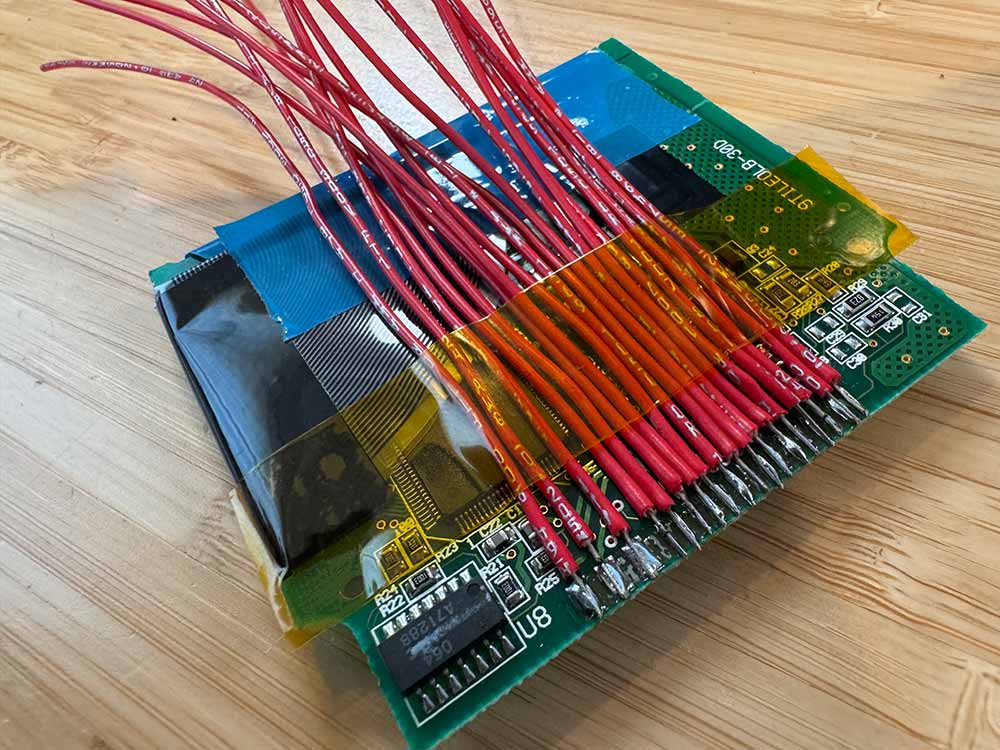
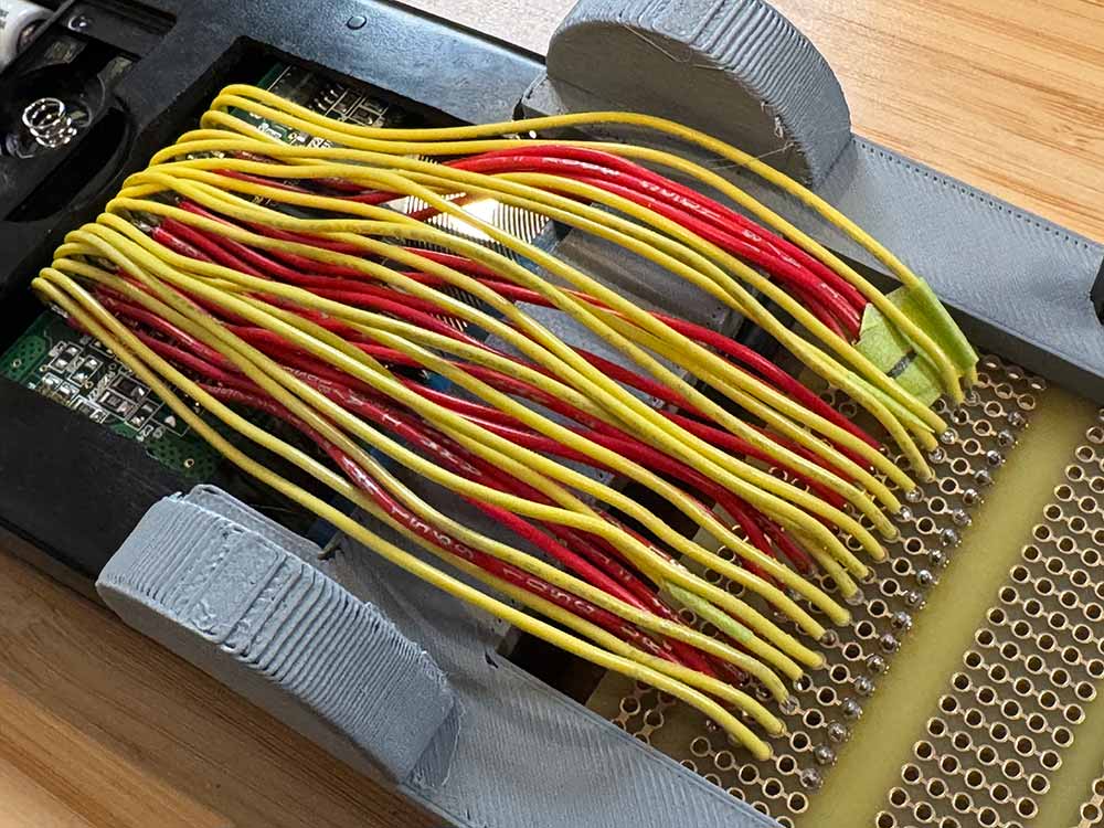
Cracking open the calculator case, we have our first bit of info: there are 18 conductors in the ribbon cable. Maybe some kind of parallel interface? Let’s see if anyone else on the Internet has blazed a trail and identified what they are.
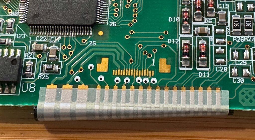
18 conductors in the display ribbon cable. This is the cable as it lands on the display PCB.
Unfortunately, there isn’t a ton of information out there. I did find three super useful sites though. Huge credit to these pioneers for sharing their work.
WikiTI
A wiki for programmers and hardware hackers of TI calculators. The documentation of the ASIC and LCD controller were a solid start. The ASIC is sending a continuous stream of pixel data to the controller. There are 128 columns and 64 rows per frame.
Vintage Z80 Palmtop Compy Hackery
Amazing – an entire hardware project focused on the TI-86! The post Inside the TI-86 was a helpful walkthrough of the overall architecture. The next post on TI-86 LCD Interfacing goes into a bit more detail on how the display might work. There is a Toshiba T6A40 chip as a row driver and a Toshiba T6A23 chip for the column driver. While the exact nature of the conductors wasn’t determined, we are now hot on the trail. From the author:
“That’s apparently what the TI-86’s CPU sends to the LCD, very similarly to VGA, with something like hsync to select the next row and vsync to select the first. Thus most LCDs always have essentially two [types of] chips, row drivers and column drivers. Huge LCDs with a lot of pixels have many of these daisychained. They’re often on the ribbon cables that go to the glass. The display driver (the CPU, in this case) typically only interfaces with the first row-driver and first column-driver chips.”
DIOLUM
Wow. Just wow. This individual desoldered all the components from the PCB, then proceeded to sand and scan the circuit board to map out the traces:
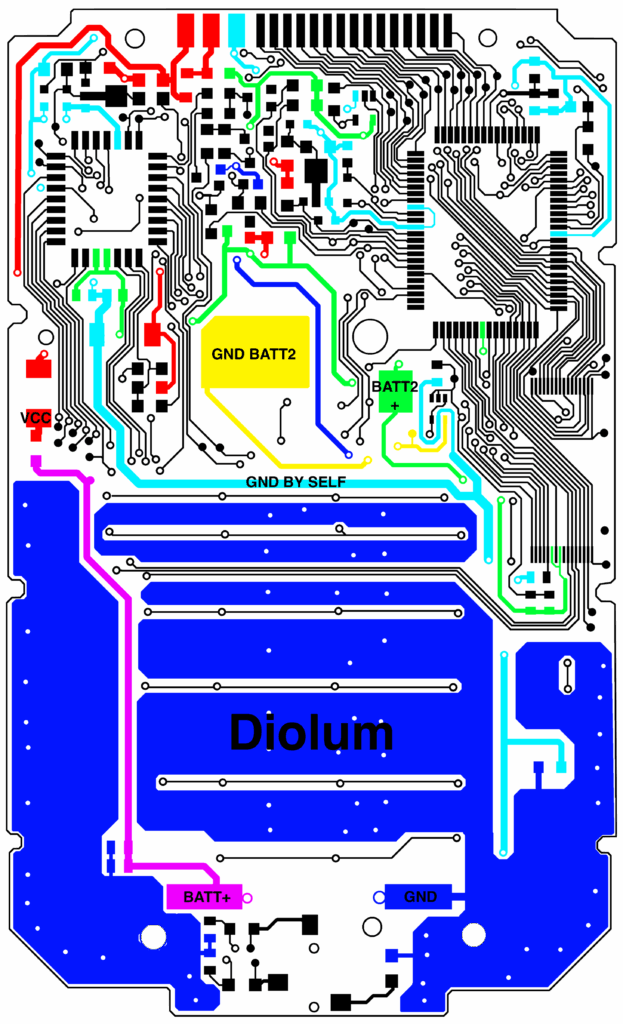
They also investigated the signals between the main PCB and the display:
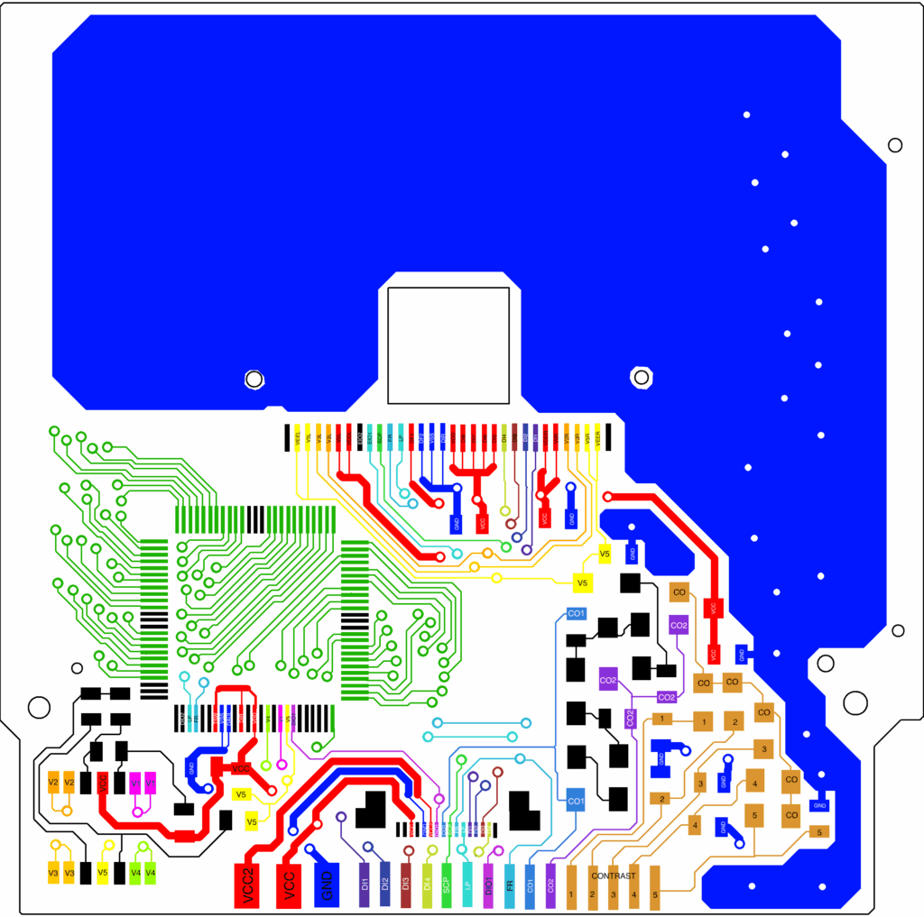
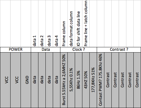
So, out of the 18 conductors, we have the following (from left to right):
- VCC2 power
- VCC1 power
- Ground
- Pixel data 1 (DI1)
- Pixel data 2 (DI2)
- Pixel data 3 (DI3)
- Pixel data 4 (DI4)
- Frame column (SCP)
- Data format column (LP)
- IO for shift data line (DIO1)
- Frame line + latch column (FR)
- Contrast PWM?
- Contrast PWM?
- Contrast level 1
- Contrast level 2
- Contrast level 3
- Contrast level 4
- Contrast level 5
Unfortunately, the Diolum investigation stopped when the author entered “Disque dur mort = perte de données et de motivation = Fin de l’ingénierie inverse (Presque)”, which translates roughly to “Dead hard drive = loss of data and motivation = End of reverse engineering (almost)”.
Crossing the Finish Line
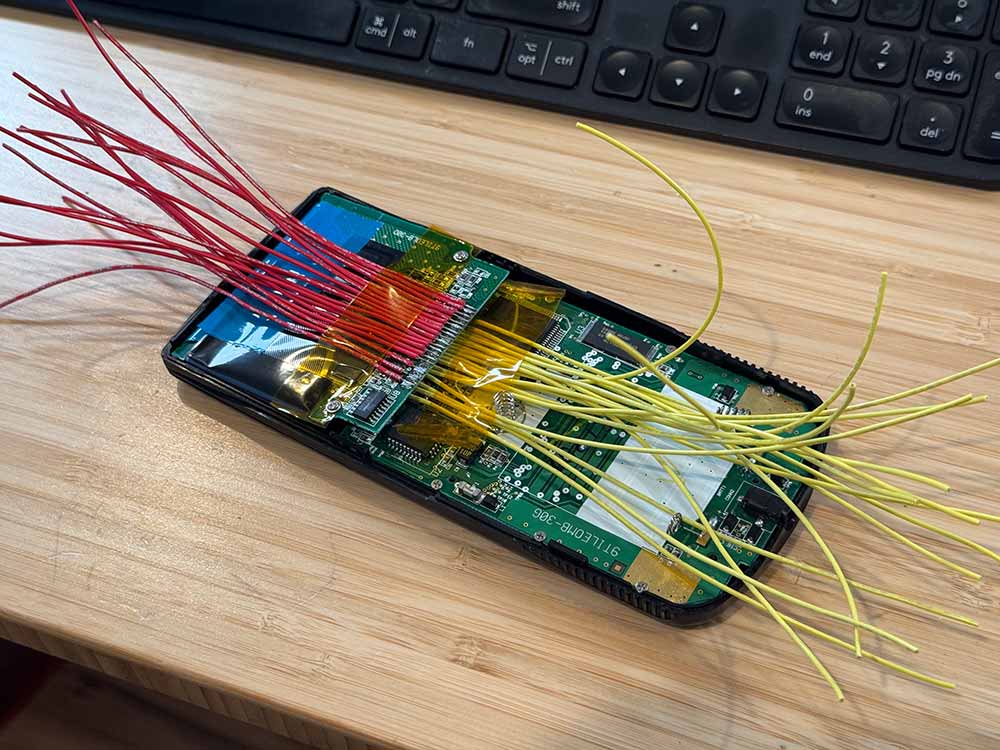
OK. While nobody has 100% cracked the code, we are set up for success. Let’s create a test rig where we can pick up where the above investigations left off. I ordered a $10 TI-86 from eBay that had bad lines on the screen and proceeded to make modifications. Our end goal here is to keep the main board connected to the screen, so we can see what is being displayed, but to break out the connections where we can easily examine the signals with an oscilloscope or digital logic analyzer.
Connecting new wires to the screen.
New wires from the mainboard and the screen, reinstalled into the calculator chassis.
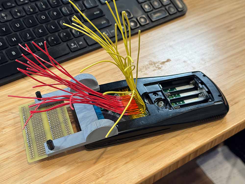
Back case reinstalled and 3D printed breadboard stand epoxied on.
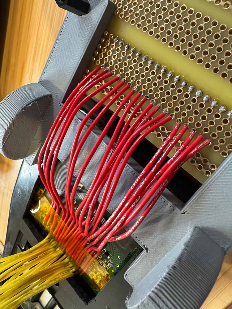
Screen wires getting connected to the breakout board.
All wires soldered to breakout board.
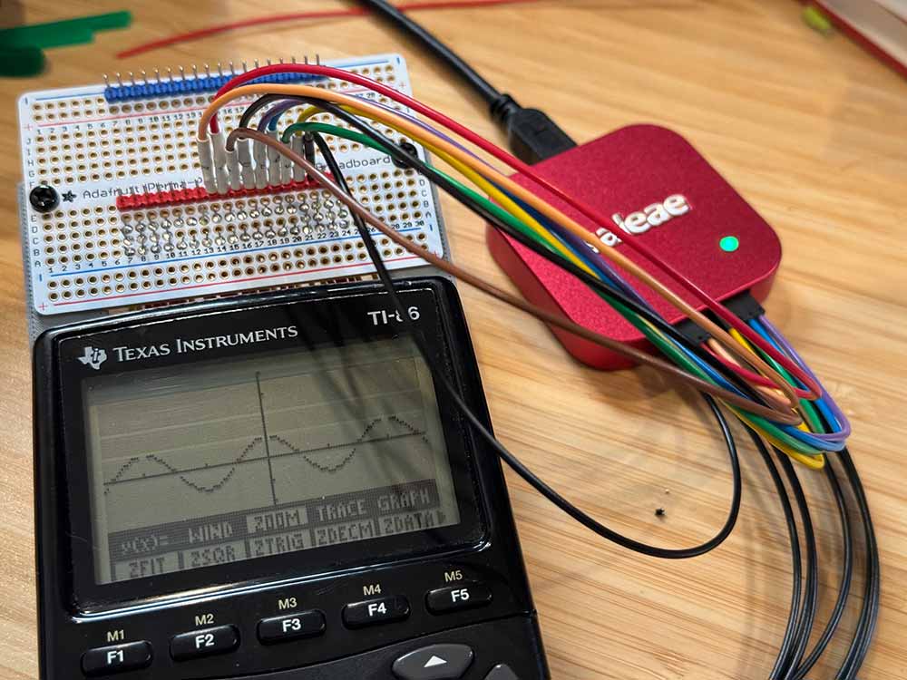
First test. It still works (to my immediate relief).
The Saleae logic analyzer was connected to the primary digital pins (#4 through #11, now right to left) and the ground. Let’s get down to reverse engineering and walk through an example frame start.
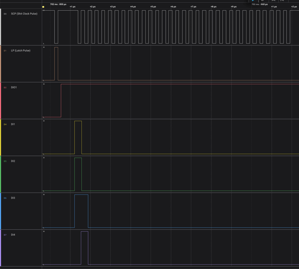
- Shift clock pulse (SCP) goes low and Latch Pulse (LP) goes high to signal a new row
- DIO1 goes high to signal the start of a frame (will remain high for first row)
- Each drop of SCP to low signals reading in the four data lines D1-D4
- Repeat 32 times to read in one row of 128 pixel values
- DI4 is read in first, followed by DI3, DI2, and DI1.
- Repeat the above for all 64 rows
From the signals in the image, you can see the following in the first 20 pixels:
-#####--------------
Now, read in the first eight lines:
-#####--------------
-#####--------------
-#####--------------
-#####--------------
-#####--------------
-#####--------------
-#####--------------
--------------------
and, what do you know: we can see the flashing cursor on the main screen:
So, we have a pretty good idea of what we need to know for the screen data protocol. We can use the DIO1 line as a signal for when a new screen/frame begins. Each row will kick off with the LP line going high. From there, each set of four bits is read in every time SCP goes low. That is enough to get going with the software on the Pi Pico. Let’s move on.